
Micron G11 NAND to hit 42 Gb/mm2
The memory maker plans to double storage density and boost I/O speeds by 50% in a late-2027 product ramp.
By Julian Kobayashi ·
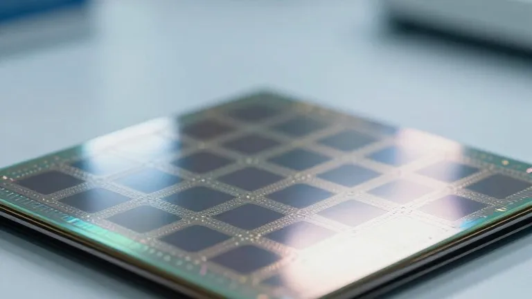
Micron Technology expects to begin mass production of its G11 generation of 3D NAND flash memory in the second half of 2027. The new chips will double storage density to 42 gigabits per square millimeter in triple-level-cell configuration, up from the current 21 gigabits per square millimeter standard.
The company detailed this roadmap at an industry event this week. Scott DeBoer, Micron’s president and chief technology and products officer, confirmed the timeline. He stated that G11 represents the right timing for specific manufacturing technologies that have been under development for several years.
Performance metrics for the G11 generation show substantial improvements over the existing G9 lineup. Input and output speeds will increase by up to 50%, rising from 3,600 megatransfers per second to 5,400 megatransfers per second. Micron also projects that the energy required to transfer each bit of data will drop by more than 25%. These efficiency gains are designed for high-capacity solid-state drives used in client devices and data centers, as well as storage solutions built for artificial intelligence workloads.
A primary engineering change in this generation is the use of wafer-on-wafer bonding. This method allows Micron to manufacture the NAND array and the peripheral circuitry on separate wafers. Each wafer is produced using a process optimized for its specific function. The two wafers are then bonded together. This approach replaces the CMOS-under-array design used in previous generations, offering greater flexibility in optimizing both the memory cells and the logic components independently.
Micron did not disclose the exact number of active wordline layers in the G11 design, though the structure will exceed 400 layers. The company attributes the density increase to a combination of additional layers and smaller memory cell dimensions. DeBoer described the design as having an industry-leading memory cell pitch. Micron plans to release further technical specifications closer to the start of high-volume production in 2027.
Beyond the G11 launch, the company indicated it will continue scaling in all three dimensions. DeBoer mentioned ongoing work with high-mobility materials and ultra-dense cell architectures. These developments aim to improve transistor characteristics and reduce internal data movement energy. Micron has not yet set specific density targets or production dates for generations following G11.
The G11 density figure of 42 gigabits per square millimeter exceeds the next-generation NAND products planned by competitors Kioxia and Samsung. Kioxia’s BiCS10 and Samsung’s V10 architectures are expected to deliver lower density figures. Micron’s move to wafer bonding aligns its manufacturing technique with that of Chinese rival YMTC, which has already adopted a similar approach.
Source: Tom's Hardware
More Business · Tech news · Consumer Watch · Report a business · Got a Story?